Source High Purity Clear Quartz Wafer for Lab, Hospital, School
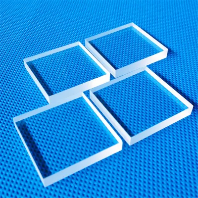
Find 30 High Purity Clear Quartz Wafer options from verified Chinese suppliers. Compare specifications including size, thickness, and polishing details for glass, casting, and metallurgy applications.
Key considerations
Products List


Quartz Wafer/Fused Silica Wafer/Quartz Glass Wafer/Semiconductor Quartz Wafer
$240.00 - $250.00
MOQ: 100 Pieces


Sapphire Glass Sheet Transparent Circular Clear Quartz Discs Quartz Wafer
$20.00 - $30.00
MOQ: 100 Pieces


Comprehensive Sourcing Guide
Strategic Sourcing Guide for High Purity Clear Quartz Wafers
Navigating the global market for high purity clear quartz wafers requires a disciplined approach that distinguishes between generic glass products and specialized semiconductor-grade substrates. The procurement landscape for these materials is defined by stringent purity requirements, specific thermal characteristics, and diverse manufacturing processes. Buyers must align their technical specifications with the actual capabilities of suppliers to ensure performance in critical applications ranging from semiconductor fabrication to high-temperature laboratory instrumentation. This guide synthesizes observed market data and technical attributes to provide a framework for evaluating potential suppliers and defining procurement requirements without relying on unverified claims.
Technical Specifications and Material Composition
The foundation of any successful procurement strategy for quartz wafers lies in a precise understanding of material composition and physical dimensions. The core material for these wafers is typically 99.9% pure SiO2, though high-end applications often demand purity levels reaching 99.99%. This distinction is critical because trace impurities can significantly alter the optical and thermal properties of the substrate. The density of the material is consistently observed around 2.2g/cm3, a standard metric that buyers should verify against incoming quality reports.
Dimensions vary widely based on the intended application. Market observations indicate size ranges from 2 inches to 6 inches, with specific standard configurations noted as 2-inch to 6-inch C-plane substrates. Thickness is another variable parameter, with observed ranges spanning from 0.1mm to 20mm in some contexts, and 0.5mm to 100mm in others. Buyers must explicitly define their required thickness tolerance, as the "customized" nature of the product allows for significant variation but requires clear communication to avoid mismatches. The shape of the wafer is generally circular, though square or round options may be available depending on the supplier's production line.
Surface finish is a decisive factor for optical and electronic performance. The surface treatment often involves polishing, which can be executed as a single-side polish or a double-side polish. For high-precision applications, double-side polishing is frequently required to ensure parallelism and surface flatness. The growth method for the crystal structure is another technical differentiator; the Ky method (Kyropoulos) is a recognized technique for growing these crystals, ensuring high structural integrity. Buyers should request detailed certificates of analysis (CoA) that confirm the specific growth method and the resulting crystal orientation.
Thermal Properties and Operational Limits
Quartz wafers are frequently selected for their ability to withstand extreme thermal environments. Understanding the thermal limits is essential for applications involving high-temperature processing. The softening point is a critical threshold, with observed values ranging from 1680°C to 1730°C. This indicates the temperature at which the material begins to deform under its own weight. For operational safety, the operating temperature is often cited around 1250°C, which is well below the softening point but represents the upper limit for sustained use.
Other thermal constants include the annealing point, observed at 1210°C, and the strain point at 1120°C. These values define the temperature ranges where internal stresses are relieved or where the material transitions from a rigid to a more viscous state. When sourcing wafers for processes involving rapid thermal cycling, buyers must ensure the supplier can guarantee these thermal parameters. The "customized" standard mentioned in market listings suggests that thermal performance can be tailored, but the baseline values provided above serve as a reference for high-purity grades. Any deviation from these thermal characteristics should be treated as a potential red flag unless explicitly justified by a specific, lower-grade application.
Compliance, Certification, and Quality Standards
In the B2B procurement of specialized materials, compliance is as important as the physical product. The most frequently observed certifications for quartz wafers in the current market are ISO and CE. These certifications indicate that the supplier adheres to international management standards and European safety directives, respectively. However, buyers should not assume that every listed product carries these certifications without verification. The presence of ISO certification is a strong indicator of a mature quality management system, while CE marking is essential for products entering the European market.
Beyond general certifications, specific industry standards must be verified. The market lists standards such as "2inch to 6 inch Cplane," which refers to the crystallographic orientation of the wafer. This is a technical standard rather than a commercial one, and it dictates how the wafer behaves under specific physical forces. Buyers must confirm that the "customized" standard offered by a supplier aligns with their specific engineering drawings. Additionally, the origin of the product is a key compliance factor. Major production hubs identified include Lianyungang, Henan, and Jiangsu in China. While these locations are known for quartz processing, buyers should verify the specific factory location to ensure supply chain transparency and to assess any geopolitical or logistical risks associated with the origin.
Cost Drivers and Pricing Dynamics
The pricing of high purity clear quartz wafers is influenced by a complex interplay of factors, including purity levels, dimensions, surface finish, and order volume. The observed price range in the market is vast, spanning from $0.01 to $1000 per unit. This extreme variance reflects the difference between raw stock, standard off-the-shelf items, and highly customized, high-purity wafers. A price at the lower end of this spectrum likely corresponds to lower purity grades, smaller sizes, or less rigorous surface finishing. Conversely, prices approaching the upper limit are associated with 99.99% purity, large diameters (6 inches), and double-side polishing.
Minimum Order Quantity (MOQ) is another significant cost driver. The observed MOQ range is 1 to 100 units. For prototyping or small-batch research, suppliers offering an MOQ of 1 are valuable, though the unit cost will be higher. For mass production, negotiating an MOQ closer to 100 or higher can yield significant economies of scale. The "customized" nature of the product also impacts cost; any deviation from standard sizes or shapes incurs additional setup and processing fees. Buyers should request a detailed cost breakdown that separates material costs from processing fees, such as polishing and cutting, to understand the true value proposition.
Typical Applications and Use Cases
The versatility of high purity clear quartz wafers makes them suitable for a diverse array of industries. The primary application sectors identified include laboratory, hospital, and school environments, where the material is used for high-precision instrumentation and optical components. In industrial settings, the applications extend to glass manufacturing, casting, metallurgy, and chemical processing. The material's resistance to thermal shock and chemical corrosion makes it ideal for use in furnaces, crucibles, and reaction vessels.
Specific use cases depend heavily on the technical specifications. In the semiconductor industry, the C-plane orientation and high purity are critical for photolithography and wafer processing. In the chemical industry, the transparency and inertness of the quartz allow for visual monitoring of reactions in high-temperature vessels. The "Glass" application is listed as a distinct category, suggesting use in optical lenses or specialized glass components. Buyers must map their specific process requirements to the material properties; for instance, a process requiring operation at 1250°C necessitates a wafer with a confirmed annealing point well above that threshold to prevent structural failure.
Supplier Evaluation and Quality Control
Evaluating a supplier for quartz wafers requires a multi-faceted approach that goes beyond price comparison. The first step is verifying the supplier's capability to meet the specific technical standards. Buyers should request samples to test the physical and optical properties firsthand. The market data indicates that samples are generally available, which is a positive indicator of supplier confidence. When evaluating samples, focus on the surface finish (single vs. double side polished), the thickness tolerance, and the clarity of the material.
Packaging is a critical, often overlooked aspect of quality control. The observed packaging methods range from wooden boxes and standard export packages to inner bubble film with cartons. For high-value wafers, the packaging must provide adequate protection against vibration and impact during transit. A supplier offering "individual packaging" or "25PCS packaging" demonstrates a higher level of care in handling fragile items. Additionally, the supplier's location and logistics capabilities should be assessed. Origins in Lianyungang, Henan, and Jiangsu suggest established supply chains, but buyers should verify lead times, which can vary. A standard lead time of 2 weeks is observed, but customized orders may require longer durations.
Long-Term Procurement Considerations
Sourcing high purity quartz wafers is not a one-time transaction but a long-term partnership that requires ongoing quality assurance. Customization is a key feature of the market, with suppliers offering tailored solutions for length, thickness, and standard specifications. This flexibility is beneficial for buyers with unique requirements but necessitates clear communication and documentation to ensure consistency across batches. Buyers should establish a quality agreement that defines acceptable tolerances for thickness, surface roughness, and purity levels.
Sustainability and supply chain resilience are also important considerations. The processing services listed, such as welding, punching, decoiling, cutting, and molding, indicate that suppliers may offer value-added services. Integrating these services into the procurement strategy can reduce the number of vendors required. However, buyers must ensure that these additional processes do not compromise the integrity of the quartz material. Finally, maintaining a relationship with a supplier that offers ISO and CE certifications provides a layer of security regarding compliance and quality management. Regular audits and performance reviews should be part of the long-term strategy to ensure that the supplier continues to meet the evolving needs of the buyer's production processes.
| Feature | Observation | Buyer Verification Action |
|---|---|---|
| Purity | 99.9% to 99.99% SiO2 | Request Certificate of Analysis (CoA) |
| Certification | ISO, CE | Verify current certificate validity |
| Dimensions | 2-6 inch, 0.1-100mm thickness | Confirm specific tolerance requirements |
| Surface | Single/Double Side Polished | Inspect sample for flatness and roughness |
| Thermal | Softening 1680-1730°C | Match to process temperature limits |
| Packaging | Wooden Box, Bubble Film, Carton | Ensure protection for fragile wafers |
| Origin | China (Lianyungang, Henan, Jiangsu) | Verify factory location and logistics |
FAQs
What is the typical purity level for high purity clear quartz wafers?
The typical purity level ranges from 99.9% to 99.99% pure SiO2. Buyers should verify the specific grade via a Certificate of Analysis, as trace impurities can alter optical and thermal properties for critical applications.
How is the surface finish of quartz wafers typically treated?
Surface treatment usually involves polishing, available as single-side or double-side polished. Double-side polishing is often required for high-precision applications to ensure parallelism and surface flatness for electronic performance.
Can suppliers provide samples for testing before bulk orders?
Yes, samples are generally available for testing physical and optical properties. Buyers should request samples to verify surface finish, thickness tolerance, and material clarity before committing to larger customized orders.
What certifications are commonly observed for quartz wafer suppliers?
ISO and CE certifications are the most frequently observed standards in the market. These indicate adherence to international management systems and European safety directives, though buyers must verify specific product compliance.
Which thermal limits should be considered for high-temperature applications?
Operating temperatures are often cited around 1250°C with softening points between 1680°C and 1730°C. Buyers must ensure the annealing point exceeds their process temperature to prevent structural failure during thermal cycling.
What are the standard size ranges for quartz wafers available?
Standard sizes range from 2 inches to 6 inches, often in C-plane configurations. Thickness varies from 0.1mm to 20mm or up to 100mm depending on the specific customization and application requirements.
How does customization affect the lead time and cost?
Customization impacts both cost and lead time, with standard lead times around 2 weeks. Deviations from standard sizes or shapes incur setup fees and may extend the duration beyond the typical shipping window.