Source Polished Cz Silicon Wafer for Solar, LED, and Sensors
Find 30 verified listings for Polished Cz Silicon Wafer options suitable for solar cells, LED manufacturing, and sensor fabrication. Buyers can compare specifications like diameter, thickness, and surface finish across multiple suppliers to select the right material grade.
Key considerations
Products List






Comprehensive Sourcing Guide
Strategic Sourcing Guide for Polished CZ Silicon Wafers
Navigating the procurement landscape for polished Czochralski (CZ) silicon wafers requires a disciplined approach that balances technical precision with supply chain reliability. These wafers serve as the foundational substrate for a vast array of semiconductor devices, from power electronics to integrated circuits. The sourcing process is not merely about purchasing a commodity; it involves verifying complex material properties, surface finishes, and dimensional tolerances that directly impact device yield and performance. Buyers must distinguish between various grades, orientations, and dopant types while ensuring that the selected supplier can consistently meet the rigorous demands of modern semiconductor manufacturing. This guide outlines the critical factors for evaluating polished CZ silicon wafers, focusing on the specific attributes observed in the current market, including diameter ranges, surface quality metrics, and origin considerations.
Technical Specifications and Material Attributes
The core of any procurement decision for silicon wafers lies in the precise definition of technical specifications. The material itself is an element semiconductor, typically sourced in a Prime grade, which indicates high purity suitable for advanced fabrication processes. The growth method is predominantly Czochralski (CZ), a technique that allows for the production of large-diameter crystals with controlled impurity levels. However, buyers must also be aware of the existence of alternative growth methods such as Float Zone (FZ) in certain product lines, which offer different electrical characteristics. The crystal orientation is a critical parameter, with common orientations including (100) +/-0.5 degrees and (111), each serving distinct purposes in device fabrication. The (100) orientation is often preferred for MOSFETs due to its favorable interface properties, while (111) is sometimes utilized for specific bipolar applications.
Doping is another essential variable. The market offers both P-Type and N-Type variants, with specific dopants such as Boron (B) for P-Type and Phosphorus or Arsenic for N-Type. The resistivity range is equally critical, with observed specifications spanning from 0.0005 to 150 Ohm-cm. This wide range accommodates everything from highly conductive substrates to high-resistivity isolators. The physical dimensions of the wafer are equally standardized yet customizable. Observed diameter specifications range from 3 mm to 150 mm, with a specific tolerance of +0.0/-0.15 mm for the diameter. Thickness is typically around 525 micrometers with a tolerance of +/-25 micrometers, though this can vary based on the specific model and application requirements. The surface finish is a defining characteristic of the "polished" designation, with options for double-side polishing or single-side polishing. Surface quality is often quantified by scratch-dig standards, such as 60/40 or 40/20, indicating the allowable density of defects on the surface.
Dimensional Tolerances and Surface Quality Metrics
Precision in dimensional control is paramount for automated handling in semiconductor fabrication lines. The thickness tolerance of +/-0.1 mm for some glass-based substrates or specific silicon variants highlights the need for tight control over wafer flatness. For silicon wafers, the Total Thickness Variation (TTV) is a key metric, with observed standards requiring TTV to be less than 15 micrometers. Similarly, Bow and Warp are critical for ensuring the wafer remains flat during processing. Observed data indicates that Bow should be less than 30 micrometers and Warp less than 65 micrometers. These metrics ensure that the wafer does not deform under the thermal stresses of lithography or deposition processes.
Surface quality is further defined by particle counts. High-grade wafers must maintain particle counts below 30 particles at a 0.3-micrometer size threshold. This stringent requirement is necessary to prevent defects that could compromise the integrity of thin films or circuit patterns. The surface finish, whether double-side polished or single-side polished, directly influences the downstream processing steps. Double-side polishing is often required for applications demanding extreme flatness, while single-side polishing may suffice for specific power device applications. Buyers must verify that the supplier's surface quality claims align with the specific requirements of their manufacturing process, as even minor deviations in surface roughness can lead to significant yield losses.
Compliance, Certification, and Origin Verification
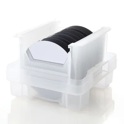
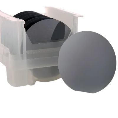
When sourcing silicon wafers, verifying the origin and compliance of the product is as important as the technical specifications. The supply chain for these materials is global, with significant production hubs located in regions such as Changchun and Jiaozuo in Henan. The origin of the wafer can influence the consistency of the material properties and the reliability of the supply chain. Buyers should explicitly request and verify the production origin to ensure it aligns with their risk management strategies. Furthermore, the packaging standards are crucial for maintaining the integrity of the wafers during transit. Observed packaging options include standard cartons, safety green cartons, and specialized boxes, each designed to protect the delicate surfaces from contamination and physical damage.
Compliance and certification checks are essential to ensure that the wafers meet industry standards. While specific certification names are not universally mandated for all silicon wafers, the adherence to standards such as the 0.1-300mm range for product specifications suggests a need for standardized measurement protocols. Buyers should verify that the supplier adheres to recognized industry standards for semiconductor materials. The presence of a batch number, such as "Polished," indicates traceability, which is a critical component of quality assurance. Additionally, the brand reputation, such as Finewen, can serve as a proxy for quality consistency, though buyers should not rely solely on brand names without verifying the specific product attributes. It is vital to ensure that the supplier can provide documentation confirming the material grade, growth method, and surface quality metrics.
Cost Drivers and Pricing Dynamics
The pricing of polished CZ silicon wafers is influenced by a complex interplay of factors, including diameter, thickness, surface quality, and dopant type. The observed price range in the market spans from $0.01 to $100, reflecting the vast diversity in product specifications. Smaller diameters or lower-grade materials may fall at the lower end of this spectrum, while large-diameter, high-precision wafers with double-side polishing and tight tolerances command premium prices. The Minimum Order Quantity (MOQ) also plays a significant role in cost dynamics, with observed ranges from 1 to 100 units. Buyers must balance their volume requirements against the unit cost to optimize their procurement strategy.
Customization is a major cost driver. Products offering customized dimensions, orientations, or surface finishes often come at a higher price point due to the specialized processing required. The availability of customization options, such as specific dopant concentrations or unique packaging, allows buyers to tailor the product to their exact needs but may increase the lead time and cost. Additionally, the origin of the wafer can impact pricing due to logistics, tariffs, and regional labor costs. Buyers should request detailed cost breakdowns to understand the components of the final price, including material costs, processing fees, and packaging expenses. Understanding these drivers enables more effective negotiation and budget planning.
Typical Applications and Performance Requirements
Polished CZ silicon wafers are integral to a wide range of semiconductor applications, with the LED industry being a prominent example. The specific model numbers, such as yt953, yt970, and FW-Silicon, often correspond to specific application profiles. For instance, wafers with high resistivity and specific orientations are ideal for power devices, while those with lower resistivity and specific dopant levels are suited for integrated circuits. The intrinsic semiconductor type is also relevant for applications requiring high purity and low defect densities. The choice of wafer depends heavily on the intended device performance, such as the breakdown voltage, switching speed, or thermal conductivity.
Buyers must align the wafer specifications with their application requirements. For example, a wafer with a (100) orientation and double-side polish is often preferred for CMOS processes, while a (111) orientation might be selected for specific bipolar junction transistors. The thickness and diameter must also match the processing equipment capabilities. A mismatch in these parameters can lead to processing errors or equipment damage. Furthermore, the surface quality and particle count are critical for high-density integration, where even microscopic defects can cause circuit failures. Understanding the specific performance requirements of the target application ensures that the selected wafer will deliver the desired results in the final device.
Supplier Evaluation and Quality Control Protocols
Evaluating suppliers for polished CZ silicon wafers requires a rigorous assessment of their manufacturing capabilities and quality control systems. Buyers should look for suppliers who demonstrate a clear understanding of the growth methods, such as CZ and FZ, and can provide detailed data on their crystal growth processes. The ability to maintain tight tolerances on diameter, thickness, and surface quality is a key indicator of supplier competence. Suppliers should be able to provide test results for key metrics such as TTV, Bow, Warp, and particle counts. The presence of a batch number system and traceability protocols is also essential for ensuring quality consistency.
Quality control protocols should include regular inspections of surface finish, dimensional accuracy, and material purity. Buyers should request samples or test reports to verify that the supplier's claims match the actual product attributes. The packaging method, whether it is a standard carton, safety green carton, or box, should be evaluated for its ability to protect the wafers during shipping. Additionally, the supplier's ability to handle customized orders and provide technical support is a valuable asset. A supplier with a strong track record in the industry, such as those associated with brands like Finewen, may offer additional assurance of quality and reliability. However, buyers should always verify the specific product attributes rather than relying solely on brand reputation.
Long-Term Procurement Considerations
Sourcing polished CZ silicon wafers is a long-term commitment that requires careful planning and relationship management. Buyers should consider the scalability of the supplier's production capabilities to ensure they can meet future demand. The lead time for customized orders and the flexibility of the supplier to adjust to changing requirements are also critical factors. Establishing a strong partnership with a reliable supplier can help mitigate supply chain risks and ensure a steady flow of high-quality materials.
Buyers should also monitor market trends and technological advancements in the semiconductor industry. As device requirements evolve, the specifications for silicon wafers may change, necessitating a proactive approach to procurement. Regular communication with suppliers to discuss potential improvements or new product offerings can help buyers stay ahead of the curve. Additionally, maintaining a diverse supplier base can provide redundancy and reduce the risk of supply disruptions. By focusing on long-term strategic planning, buyers can ensure a stable and efficient supply chain for their semiconductor manufacturing needs.
FAQs
What growth methods are used for polished CZ silicon wafers?
The primary growth method is Czochralski (CZ), though some products also utilize Float Zone (FZ) techniques. This distinction affects electrical properties, with CZ offering large diameters and FZ providing higher purity for specific high-resistivity applications.
Which crystal orientations are available for these silicon wafers?
Common orientations include (100) with a tolerance of plus or minus 0.5 degrees and (111) orientations. The (100) orientation is often preferred for MOSFETs, while (111) is sometimes selected for specific bipolar device applications.
Can buyers request customized dimensions and surface finishes?
Yes, customization is available for dimensions, orientations, and surface finishes like double-side polishing. Buyers can specify unique requirements such as specific dopant concentrations or packaging types to tailor the product to their exact manufacturing needs.
What is the typical thickness tolerance for these wafers?
The standard thickness is approximately 525 micrometers with a tolerance of plus or minus 25 micrometers. Some specific variants may have tighter tolerances around 0.1 millimeters depending on the model and intended application requirements.
How are surface quality and particle counts defined for these wafers?
Surface quality is often graded as 60/40 or 40/20, indicating allowable scratch and dig densities. High-grade wafers must maintain particle counts below 30 particles at a 0.3-micrometer size threshold to ensure defect-free processing.
Which locations produce these polished silicon wafers?
Production origins include Changchun and Jiaozuo in Henan province. Verifying the specific origin is crucial for supply chain reliability and ensuring the material properties align with your risk management and quality assurance strategies.
What packaging options are provided for these semiconductor wafers?
Packaging options include standard cartons, safety green cartons, and specialized boxes designed to protect delicate surfaces. The choice of packaging ensures the wafers remain free from contamination and physical damage during transit to the buyer.